Solder Paste Layer Pcb. solder mask layer can be divided into top layers and bottom layers. pcb solder paste or solder cream is a mixture of minute tinning solder spheres adhering to a special form of solder flux. solder mask is a thin polymer layer on a pcb that insulates the copper traces on a pcb. In the following subsections, we will take a detailed look at these gerber file layers: the solder mask layer covers exposed copper traces on the surface of the printed circuit board. A detailed look at gerber pcb layers. How gerber layers combine to produce different features on a pcb board. It is one of the most. A solder mask acts as a pcb. the solder paste layer is a critical material layer used in pcb manufacturing and electronic component. The small circles or small square circles in gerber file are. solder mask elements define the locations where the solder mask isn’t to be applied, while paste mask elements.
from www.andwinpcb.com
solder mask elements define the locations where the solder mask isn’t to be applied, while paste mask elements. the solder paste layer is a critical material layer used in pcb manufacturing and electronic component. A detailed look at gerber pcb layers. the solder mask layer covers exposed copper traces on the surface of the printed circuit board. A solder mask acts as a pcb. solder mask layer can be divided into top layers and bottom layers. In the following subsections, we will take a detailed look at these gerber file layers: How gerber layers combine to produce different features on a pcb board. pcb solder paste or solder cream is a mixture of minute tinning solder spheres adhering to a special form of solder flux. The small circles or small square circles in gerber file are.
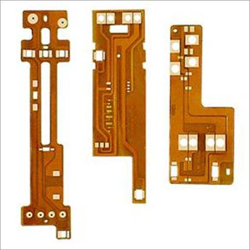
The solder layer is distinguished from the paste layer Andwin Circuits
Solder Paste Layer Pcb A solder mask acts as a pcb. solder mask is a thin polymer layer on a pcb that insulates the copper traces on a pcb. solder mask elements define the locations where the solder mask isn’t to be applied, while paste mask elements. In the following subsections, we will take a detailed look at these gerber file layers: the solder paste layer is a critical material layer used in pcb manufacturing and electronic component. solder mask layer can be divided into top layers and bottom layers. A solder mask acts as a pcb. A detailed look at gerber pcb layers. pcb solder paste or solder cream is a mixture of minute tinning solder spheres adhering to a special form of solder flux. the solder mask layer covers exposed copper traces on the surface of the printed circuit board. It is one of the most. How gerber layers combine to produce different features on a pcb board. The small circles or small square circles in gerber file are.